
ZVS Buck Converter with Variable-Step MPPT
Background and Motivation
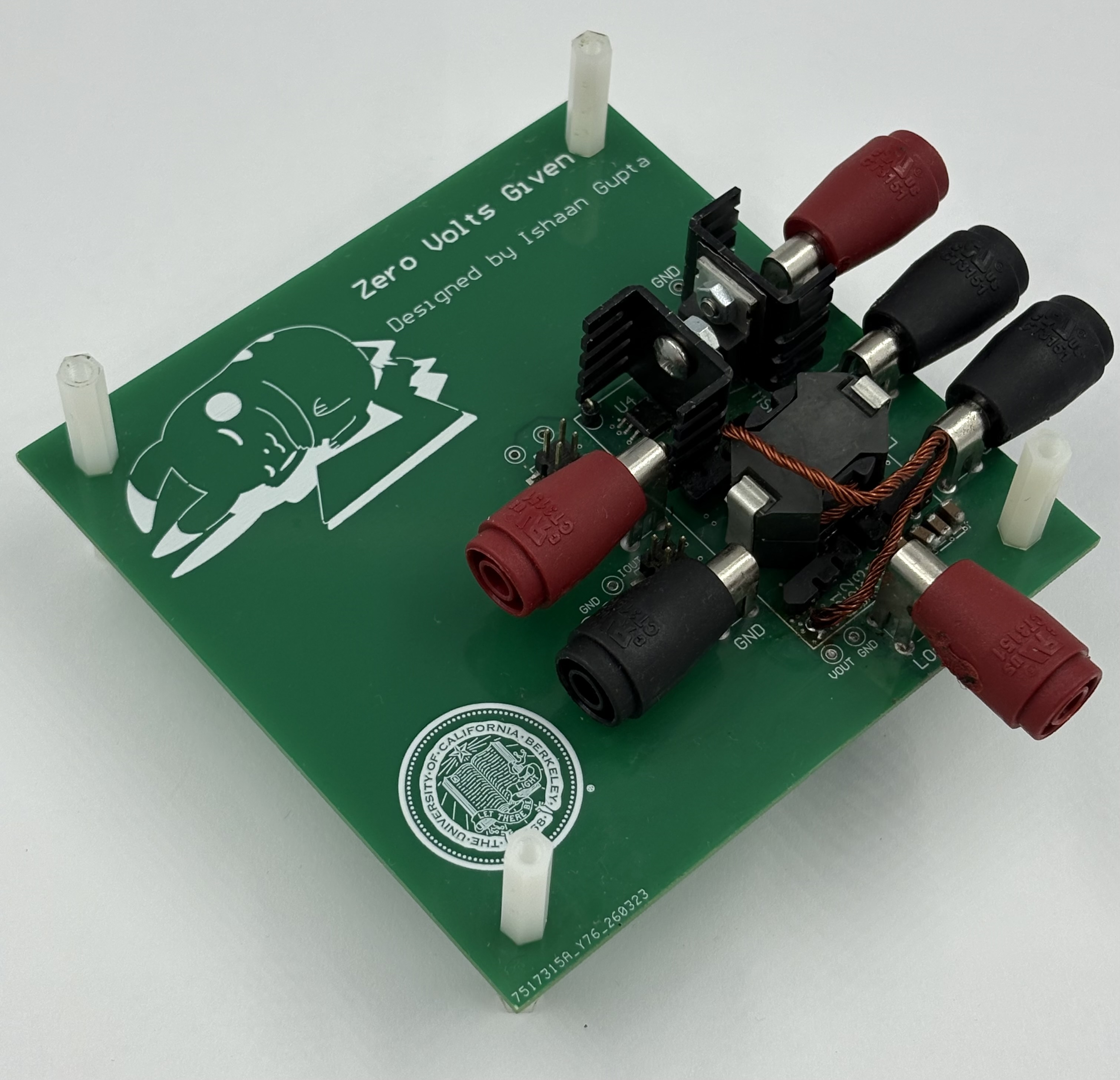
For EE 113B: Power Electronics Design at UC Berkeley, I designed, built, and tested a DC-DC resonant-transition synchronous buck converter with variable-step maximum power point tracking (MPPT). The application was charging a 12 V battery from a solar panel whose available voltage and power change with solar irradiance.
The challenge was to maintain zero-voltage switching (ZVS) while moving the panel toward its maximum power point. That brought together power-stage design, custom AC magnetics, PCB layout, sensing, and embedded control—and made this project a practical introduction to the tradeoffs of soft switching.
| Design specification | Target |
|---|---|
| Input voltage | 16–24 V |
| Output voltage | 12 V |
| Nominal operating point | 20 V input, 100 W output |
| Output power range | 50–100 W |
| Input and output voltage ripple | Below 5% |
| Inductor current ripple | Above 200% to enable ZVS |
Converter Topology
A synchronous buck converter uses two MOSFETs to step down the input voltage. In this resonant-transition implementation, the output inductor also exchanges energy with the MOSFETs’ output capacitances during the deadtime between switching events.
I deliberately designed for enough current ripple to drive the inductor current negative. That negative current discharges the high-side MOSFET’s output capacitance before turn-on, allowing it to switch at approximately zero drain-to-source voltage. The tradeoff is higher circulating current and conduction loss in exchange for reduced switching loss.
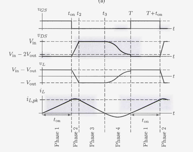
Because the input voltage and load vary, a single switching frequency cannot preserve the desired current ripple across the operating range. Duty cycle controls the solar panel operating point, while switching frequency is adjusted to maintain ZVS.
Calculating the ZVS Frequency
I selected a peak-to-peak inductor-current ripple of 215% of the average output current. A ripple above 200% lets the current cross zero; the additional margin supplies the negative current needed to move charge between the two MOSFET output capacitances during deadtime.
\[I_{\mathrm{out}}=\frac{P_{\mathrm{out}}}{V_{\mathrm{out}}},\qquad I_{L,\mathrm{pk}}=I_{\mathrm{out}}+\frac{\Delta I_{L,\mathrm{pp}}}{2}\]My resonant-transition timing model adds the two linear current-ramp intervals and the resonant transition interval:
\[f_{\mathrm{ZVS}}=\left( \frac{L I_{L,\mathrm{pk}}}{V_{\mathrm{in}}-V_{\mathrm{out}}} +\frac{L I_{L,\mathrm{pk}}}{V_{\mathrm{out}}} +\pi\sqrt{2LC_{\mathrm{oss}}} \right)^{-1}\]Here, the factor of two accounts for the output capacitances of both MOSFETs, using an equal-capacitance approximation. This timing model provides a design estimate; the final controller uses experimentally calibrated PWM periods.
The negative-current requirement follows from the charge that must be transferred during the high-side turn-on deadtime. Approximating the transition current as triangular gives:
\[\frac{1}{2}I_{\mathrm{neg,min}}t_{\mathrm{ZVS}} =2C_{\mathrm{ossQ}}V_{\mathrm{in}},\qquad I_{\mathrm{neg,min}}=\frac{4C_{\mathrm{ossQ}}V_{\mathrm{in}}}{t_{\mathrm{ZVS}}}\] \[\Delta I_{L,\mathrm{pp,min}}=2\left(I_{\mathrm{out}}+I_{\mathrm{neg,min}}\right)\]\(C_{\mathrm{ossQ}}\) denotes the charge-equivalent output capacitance used for sizing. The report estimated a 336 ns transition interval; bench tuning led to a 350 ns deadtime. This interval is distinct from the full switching period.
| Operating point | Calculated switching frequency |
|---|---|
| 20 V, 100 W (nominal) | 141 kHz |
| 16 V, 50 W | 91 kHz |
| 16 V, 100 W | 182 kHz |
| 24 V, 50 W | 155 kHz |
| 24 V, 100 W | 315 kHz |
Inductance and Capacitance Sizing
With the required current ripple established, I used the buck converter’s on-time current slope to size the inductor. At each sizing point, duty cycle, input voltage, ripple, and switching frequency must refer to the same operating condition:
\[D\approx\frac{V_{\mathrm{out}}}{V_{\mathrm{in}}},\qquad \Delta I_{L,\mathrm{pp}}=\frac{D(V_{\mathrm{in}}-V_{\mathrm{out}})}{Lf_{\mathrm{sw}}}\] \[L=\frac{D(V_{\mathrm{in}}-V_{\mathrm{out}})}{\Delta I_{L,\mathrm{pp}}f_{\mathrm{sw}}}\]Input capacitance buffers the pulsed current drawn by the switching stage. Output capacitance absorbs the inductor-current ripple and the charge associated with the resonant transitions. My report used the following minimum-capacitance estimates, with voltage ripple expressed as peak-to-peak volts:
\[C_{\mathrm{in,min}}= \frac{I_{\mathrm{out}}D(1-D)}{\Delta V_{\mathrm{in,pp}}f_{\mathrm{sw}}}\] \[C_{\mathrm{out,min}}= \frac{4C_{\mathrm{ossQ}}V_{\mathrm{in}} +\dfrac{\Delta I_{L,\mathrm{pp}}}{8f_{\mathrm{sw}}}} {\Delta V_{\mathrm{out,pp}}}\]The input expression is a first-order buck sizing estimate. The output expression combines a transition-charge allowance with triangular current ripple. I evaluated sizing across the operating range, with ripple limits of 5% of input and output voltage. The 16 V, 50 W corner has the lowest listed switching frequency, making it an important filter-sizing condition.
| Sizing result | Value |
|---|---|
| Input capacitance requirement | 19.10 µF |
| Output capacitance requirement | 40.47 µF |
| Selected inductance | 1.88 µH |
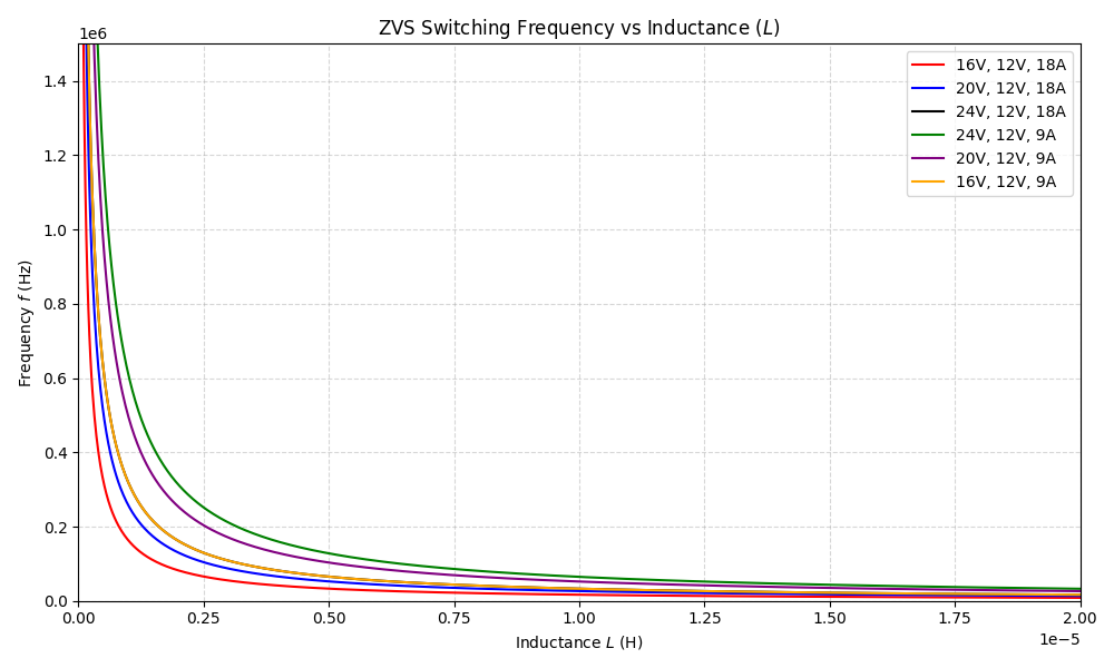
The proportionalities in my slides show why frequency and filter size have to be chosen together. At fixed duty cycle, voltage, and required current ripple:
\[f_{\mathrm{sw}}\propto\frac{1}{L},\qquad C_{\mathrm{in,min}}\propto\frac{1}{f_{\mathrm{sw}}}\]For the triangular-ripple contribution to output capacitance:
\[C_{\mathrm{out,ripple}}\propto\frac{\Delta I_{L,\mathrm{pp}}}{f_{\mathrm{sw}}},\qquad \Delta V_{\mathrm{out,pp}}\approx\frac{\Delta I_{L,\mathrm{pp}}}{8f_{\mathrm{sw}}C_{\mathrm{out}}}\]Lowering frequency can therefore increase voltage ripple or require larger capacitors. The full output-capacitance expression also includes a transition-charge term that does not scale with frequency in the same way.
I selected parallel 50 V X7R MLCCs and checked capacitance at the actual DC bias, rather than using their nominal 10 µF rating. The report lists eight capacitors per bank, with approximately 3.7 µF per capacitor at 24 V input bias and 7 µF at 12 V output bias—effective totals of 29.6 µF and 56 µF, respectively.
AC Magnetics
The inductor carries both a DC component and a substantial AC component. Designing it required balancing core loss, copper loss, size, and the switching-frequency range. More turns can reduce core loss, but increase winding resistance; high-frequency operation also makes skin and proximity effects significant.
The final inductor used a 3C95 RM8 ferrite core, five turns of eight-strand 28 AWG wire, and a 1.06 mm air gap, with a characterized inductance of 1.88 µH. I designed around the nominal operating point, then evaluated performance at the input-voltage and power corners.
This was one of the most iterative parts of the project. During bring-up, pushing the switching frequency too high caused the inductor core shims to melt. Increasing inductance reduced the required frequency, but also required more input and output capacitance to keep voltage ripple within the specification.
Core Loss, Steinmetz Relationship, and Winding Loss
The core-loss graph used in my design shows specific loss versus peak AC flux density, with frequency as a parameter. It is the 3C95 material data from the report, rather than a fitted curve for my assembled inductor. Ferroxcube material specifications provide the original core-loss data.
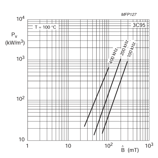
The Steinmetz relationship describes the frequency and flux-density dependence:
\[p_v\approx k f^{\alpha}\hat B^{\beta},\qquad P_{L,\mathrm{core}}=p_v V_{c,e}\]The coefficients depend on material, temperature, waveform, and operating range. My report obtained specific loss from the material curves; it did not provide fitted Steinmetz coefficients. For this converter, I estimated the AC flux excursion and winding loss using:
\[I_{\mathrm{ac}}=\frac{\Delta I_{L,\mathrm{pp}}}{2},\qquad \hat B=\frac{L I_{\mathrm{ac}}}{N A_{\min}}\] \[I_{L,\mathrm{rms}}=\sqrt{I_{\mathrm{out}}^2+\frac{\Delta I_{L,\mathrm{pp}}^2}{12}},\qquad R_w=\frac{\rho\ell_t N}{A_{w,\mathrm{act}}}\] \[P_{L,\mathrm{copper}}=R_w I_{L,\mathrm{rms}}^2,\qquad P_{L,\mathrm{total}}=P_{L,\mathrm{copper}}+P_{L,\mathrm{core}}\]Here, \(N\) is the turn count, \(A_{\min}\) the minimum core cross-section, \(V_{c,e}\) the effective core volume, \(\ell_t\) the mean length per turn, and \(A_{w,\mathrm{act}}\) the conductor cross-section. Winding resistance estimates copper loss; additional AC winding effects matter at these frequencies.
My slide’s turn-count tradeoff can be written more precisely, holding inductance, current, core geometry, frequency, and conductor cross-section fixed:
\[R_w\propto N,\qquad P_{L,\mathrm{copper}}\propto N,\qquad \hat B\propto\frac{1}{N},\qquad P_{L,\mathrm{core}}\propto\frac{1}{N^{\beta}}\]Thus, the slide’s inverse-turn-count relationship for core loss expresses a decreasing trend; the Steinmetz exponent determines the actual scaling. More turns reduce flux swing and core loss, while adding wire increases copper loss. I iterated the turn count to balance the two around 141 kHz. Above that nominal frequency, core loss rises; below it, core loss falls and copper loss becomes relatively more significant.
For a gap-dominated core, I used the following air-gap estimate:
\[g\approx\frac{\mu_0 A_{\mathrm{eff}}N^2}{L}\]Hardware and PCB Design
I designed the PCB in Altium, integrating the synchronous power stage, bootstrap gate drive, input and output filtering, and voltage and current sensing. A TI C2000 microcontroller generated complementary PWM signals with deadtime and sampled the feedback signals.
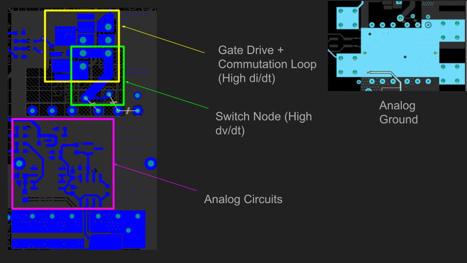
Layout focused on keeping the high di/dt commutation and gate-drive loops small, limiting the high dv/dt switch-node area, and separating the sensing circuitry from noisy power paths. I assembled and checked the board one subcircuit at a time before ramping the complete converter to full load.
View the schematic · View the PCB layout
Control: Variable-Step MPPT
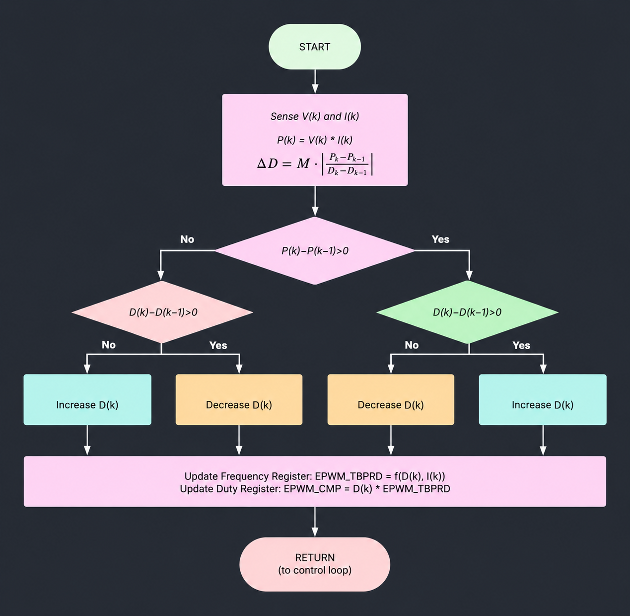
The controller uses a perturb-and-observe algorithm to search for the solar panel’s maximum power point. It measures panel voltage and current, computes power, and adjusts duty cycle based on how power changed after the previous perturbation.
Rather than using a fixed perturbation, I made the step size proportional to the magnitude of the power-versus-duty gradient. Larger steps help track a moving maximum power point; smaller steps near the peak reduce steady-state oscillation.
To coordinate MPPT with soft switching, I calibrated a lookup table of ZVS frequencies against duty cycle and output current. Bilinear interpolation supplies intermediate frequencies as the operating point changes. ADC calibration and sample averaging help make the power measurements usable for feedback.
Adaptive Step Equation
\[P_k=V_k I_k,\qquad \Delta D=M\left|\frac{P_k-P_{k-1}}{D_k-D_{k-1}}\right|\]\(M\) scales the duty-cycle perturbation. The power change and previous perturbation direction determine whether the next step increases or decreases duty cycle; the magnitude adapts to the local gradient.
ZVS Lookup Table and Interpolation
These are the experimentally calibrated TBPRD register counts from my report, indexed by duty cycle and output current. They are period values, not frequencies in kHz.
| Duty cycle / output current | 4.167 A | 5.208 A | 6.250 A | 7.291 A | 8.333 A |
|---|---|---|---|---|---|
| 0.50 | 180 | 200 | 230 | 267 | 300 |
| 0.55 | 185 | 220 | 255 | 290 | 325 |
| 0.60 | 197 | 235 | 280 | 322 | 373 |
| 0.67 | 225 | 275 | 325 | 375 | 425 |
| 0.75 | 290 | 355 | 420 | 500 | 565 |
For an operating point between four table entries, the normalized duty and current coordinates are:
\[u=\frac{D-D_i}{D_{i+1}-D_i},\qquad v=\frac{I-I_j}{I_{j+1}-I_j}\]The interpolated PWM period is:
\[\begin{aligned} Q(D,I)={}&(1-u)(1-v)Q_{i,j}+u(1-v)Q_{i+1,j}\\ &+(1-u)vQ_{i,j+1}+uvQ_{i+1,j+1} \end{aligned}\]For the C2000’s up-down counting mode, period and switching frequency are related by:
\[f_{\mathrm{sw}}=\frac{f_{\mathrm{TBCLK}}}{2\,\mathrm{TBPRD}}\]Interpolating register periods is therefore distinct from interpolating frequencies. The theoretical frequency table above explains the design range; this calibrated table supplies the hardware’s PWM settings.
The lookup table worked, but its calibration drifted between test sessions. A future version could sense the switch-node voltage directly and use that feedback to determine when each MOSFET is ready to turn on.
Results
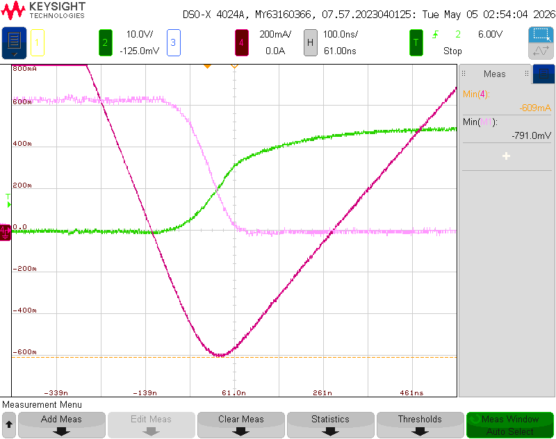
ZVS was achieved. Oscilloscope measurements verified the resonant transitions and negative inductor current, while efficiency sweeps characterized the converter across its operating range.
| Metric | Result |
|---|---|
| Weighted converter efficiency score | 88.7% |
| Average MPPT power reported in the presentation | 90.7 W |
| Power density | 2.825 W/cm³, third place |
The efficiency score weights the nominal operating point and four corner points; it is distinct from a single operating-point efficiency. The final report measured 91.1% efficiency at the nominal point and a best measured corner efficiency of 93.8%. The presentation reports 90.7 W for average MPPT power, while the report records a dynamic MPPT test score of 70.94 W.
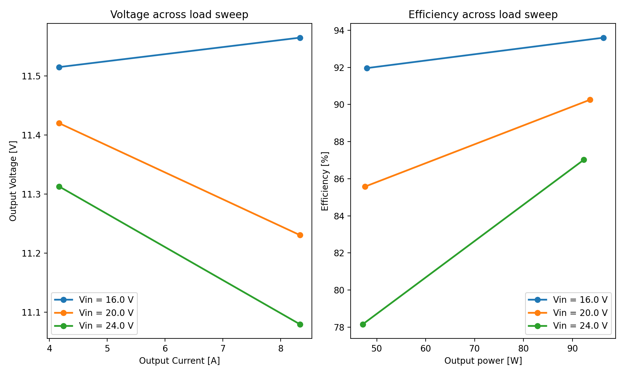
Achieving ZVS did not eliminate all losses. Measured efficiency fell below the initial model, particularly at higher input voltage. My leading explanation was excessive gate resistance: slowing the transitions helped tune the resonant timing, but extended the time the MOSFETs spent transitioning under high current. Faster gate transitions and better deadtime tuning would be priorities in a redesign.
Lessons Learned
Hardware is hard: I lost roughly eight switches and melted inductor shims while bringing this converter up. The most valuable lesson was learning how tightly coupled the design decisions were. Changing inductance affected frequency and capacitance; changing MOSFET capacitance affected resonant timing and gate-drive requirements; changing gate resistance affected losses.
Working through those dependencies taught me to test assumptions, characterize the hardware, and iterate through ambiguity. I would spend more time on the control and sensing architecture early in a redesign, especially direct feedback for ZVS timing and improved noise handling in MPPT.
This project deepened my interest in power electronics controls. I joined the Berkeley Power and Energy Center (BPEC) as a Graduate Student Researcher and want to continue pursuing work in this field.